Graphene is frequently in news recently. What is its importance? 1. It is a two-dimensional material and has good electrical conductivity 2. It is one of the thinnest but strongest materials tested so far 3. It is entirely made of silicon and has high optical transparency 4. It can be used as 'conducting electrodes' required for touch screens, LCDs and organic LEDs Which of the statements given above are correct?
Contents18
- A1 and 2 only
- B3 and 4 only
- C1, 2 and 4 only
- D1, 2, 3 and 4
Show answer
Answer: (C) 1, 2 and 4 only
Graphene is a single layer of carbon atoms arranged in a 2D hexagonal lattice.
Statement 1 correct — it is 2D and an excellent conductor of electricity.
Statement 2 correct — it is the thinnest known material (one atom thick) yet about 200 times stronger than steel.
Statement 3 is WRONG — graphene is made entirely of carbon, NOT silicon.
It does have high optical transparency, but the silicon part makes the whole statement false.
Statement 4 correct — its conductivity and transparency make it ideal for touch screens, LCDs, and OLEDs.
Graphene won the Nobel Prize in Physics in 2010.
Answer: 1, 2 and 4 only.
Graphene is a single layer of carbon atoms that is the thinnest material known (one atom thick) yet about 200 times stronger than steel.
The 2010 Nobel Prize in Physics was awarded for graphene research, making it a major science news topic around 2010-2012.
The question tests whether students can distinguish between carbon and silicon in materials science, as statement 3's silicon error is the key trap.
Graphene Structure & Properties
Science And Technology graphene two-dimensional electrical conductivity thinnest strongest
Graphene: Structure, Properties & Key Facts
Single layer of carbon atoms in hexagonal lattice — the thinnest material possible
200 times stronger than steel despite being one atom thick
Excellent electrical conductor with 97% optical transparency
Made entirely of carbon atoms, not silicon
Won Nobel Prize in Physics 2010 for isolation
What is Graphene
Graphene is a single layer of carbon atoms arranged in a 2D hexagonal lattice — essentially a one-atom-thick sheet of graphite. It represents the ultimate limit of thinness while maintaining extraordinary strength and electrical properties.
Key Properties
Property | Value/Description | Significance |
|---|---|---|
Structure | 2D hexagonal carbon lattice | Thinnest possible material |
Thickness | 0.345 nanometers (1 atom) | Truly two-dimensional |
Strength | 200x stronger than steel | Strongest material tested |
Electrical | Excellent conductor | Better than copper |
Optical | 97% transparent | Nearly invisible |
Composition | Pure carbon atoms only | Not silicon-based |
Hexagonal Structure
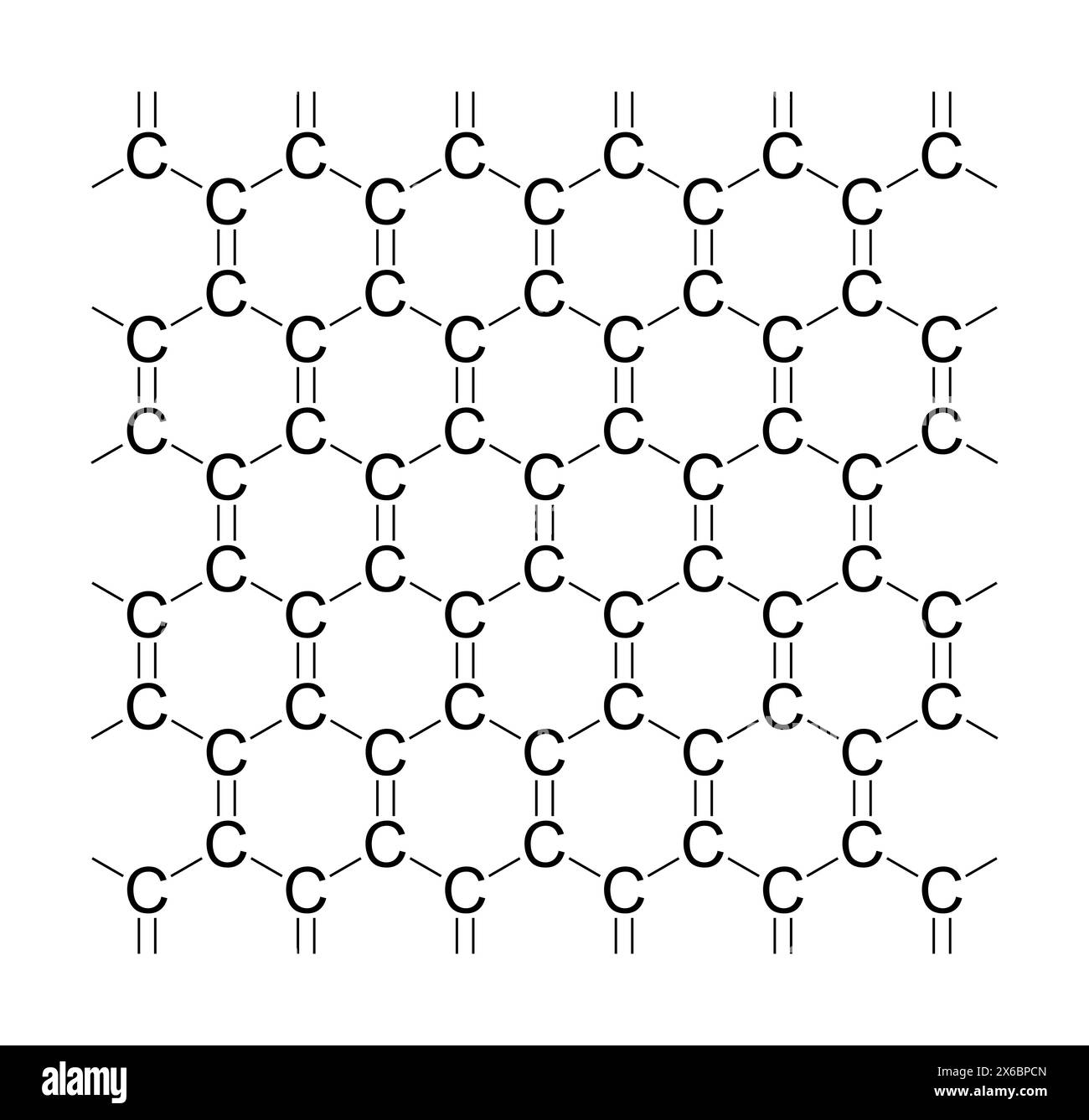
Source: Alamy — Structure of graphene. An allotrope of carbon, consisting of a ... · www.alamy.com
Question Context
This 2012 UPSC question tested basic knowledge of graphene's composition and properties. Statement 3 was the trap — graphene is made of carbon, not silicon, making that statement false despite optical transparency being correct.
Carbon vs Silicon: Graphene is pure carbon, not silicon — this is the key trap
2D doesn't mean flat: Two-dimensional means one atom thick, not a flat surface
Strength paradox: The thinnest material is also the strongest — counterintuitive but true
Transparency: High optical transparency doesn't indicate composition — silicon statement still wrong
Graphene Applications
Science And Technology conducting electrodes touch screens LCDs organic LEDs
Graphene Applications: Electronics & Display Technology
Transparent conducting electrodes for touch screens and displays
Replaces Indium Tin Oxide (ITO) in flexible electronics
Applications in LCDs, OLEDs, solar cells, and sensors
Enables flexible and bendable electronic devices
Why Graphene Works
Graphene's combination of electrical conductivity and optical transparency (97%) makes it ideal for applications requiring invisible conducting layers — exactly what touch screens and displays need.
Display Applications
Application | Role of Graphene | Advantage over Current Tech |
|---|---|---|
Touch Screens | Transparent conducting layer | More flexible than ITO |
LCDs | Transparent electrodes | Better conductivity |
Organic LEDs | Conducting electrodes | Flexibility for curved displays |
Solar Cells | Transparent front contact | Higher light transmission |
Flexible Displays | Bendable conductor | ITO cracks when bent |
Graphene Applications
# Graphene Applications
## Display Tech
- Touch Screens
- LCDs
- OLEDs
- E-paper
## Energy
- Solar Cells
- Batteries
- Supercapacitors
## Electronics
- Transistors
- Sensors
- Flexible Circuits
## Materials
- Composites
- Coatings
- Membranes
Key Advantages
Flexibility: Unlike brittle ITO, graphene can bend without breaking
Cost potential: Carbon is abundant compared to rare indium
Performance: Superior conductivity with same transparency
Scalability: Can be produced in large sheets for manufacturing
Carbon Allotropes
Science And Technology carbon silicon
Carbon Allotropes: Different Forms of Pure Carbon
Allotropes are different structural forms of the same element
Carbon has multiple allotropes: diamond, graphite, graphene, fullerenes
Same carbon atoms, different arrangements = different properties
Graphene is 2D graphite — single layer of carbon atoms
Concept of Allotropes
Allotropes are different structural arrangements of atoms of the same element. Carbon shows remarkable diversity — the same carbon atoms can form soft graphite or the hardest diamond, depending on their arrangement.
Major Carbon Allotropes
Allotrope | Structure | Key Property | Common Use |
|---|---|---|---|
Diamond | 3D tetrahedral network | Hardest natural material | Cutting tools, jewelry |
Graphite | Layered 2D sheets | Good conductor, soft | Pencil lead, electrodes |
Graphene | Single 2D sheet | Strongest + conductive | Electronics research |
Fullerenes | Hollow cage structure | Unique molecular shape | Research, medicine |
Carbon Nanotubes | Rolled graphene sheet | Very strong + light | Composites, electronics |
Carbon Structures

Source: ScienceDirect.com — Carbon Allotrope - an overview | ScienceDirect Topics · www.sciencedirect.com
Composition confusion: All carbon allotropes are pure carbon — never silicon
Property vs structure: Same element (carbon) can have opposite properties (hard diamond vs soft graphite)
Graphene-graphite relation: Graphene is one layer of graphite, not a different element
Conductivity: Diamond doesn't conduct, but graphite and graphene do excellently
2D Materials Revolution
Science And Technology two-dimensional
Two-Dimensional Materials: Beyond Graphene
2D materials are only one atom thick in one dimension
Graphene pioneered the field, leading to other 2D materials
Include transition metal dichalcogenides, borophene, silicene
Show unique properties not found in bulk materials
2D Material Concept
Two-dimensional materials are crystalline materials with thickness of just one or few atomic layers. Graphene's success opened up an entire field of 2D materials, each with unique properties.
Major 2D Materials
Material | Composition | Key Property | Potential Use |
|---|---|---|---|
Graphene | Carbon | Excellent conductor | Electronics, displays |
MoS₂ | Molybdenum disulfide | Semiconductor | Transistors, solar cells |
hBN | Hexagonal boron nitride | Electrical insulator | Substrate for electronics |
Phosphorene | Black phosphorus | Tunable bandgap | Flexible electronics |
Silicene | Silicon | Graphene-like properties | Silicon-compatible electronics |
Why 2D Materials Matter
Quantum confinement: Electrons behave differently in 2D space
Surface dominance: Almost all atoms are surface atoms
Tunable properties: Thickness change dramatically alters behavior
Stacking possibilities: Can layer different 2D materials like LEGO
2D ≠ flat surface: Two-dimensional means atomic thickness, not geometric flatness
Beyond graphene: 2D materials include insulators and semiconductors, not just conductors
Thickness matters: Adding one more atomic layer can completely change properties